Conway's Game of Life on FPGA
When learning a new programming language, I like having a well defined yet non-trivial problem to solve. Conway’s Game of Life (GoL) fits this definition. It has enough depth to uncover various tradeoffs. So naturally, when I picked up Chisel hardware description language (HDL), I wanted to build Game of Life in FPGA. It turned out to be a lot more interesting than in software. This post will follow my progress from writing Chisel and Verilog code to running GoL on Digilent Arty A7 and seeing live patterns on a VGA screen.
Chisel in a relatively new HDL originating from Berkeley and RISC V community. It uses the Scala programming language as a base and defines the HDL as a domain-specific language on top of it. In essence, Chisel is just a set of Scala libraries. This allows applying the full power of general-purpose programming language to produce higher-order hardware abstractions. This approach seems almost the opposite of how the traditional HDLs, such as Verilog, evolved. Verilog initially focused on describing the hardware–very close to what could be expressed by conventional schematic–and later added general-purpose programming elements to create more complex components.
Architecture
The trivial approach for implementing the GoL in software is to iterate over every cell. In hardware–on the contrary–the trivial approach is to have dedicated memory and compute unit for every cell. Cell units are then placed on the grid and wired to connect each to its eight neighbors. On every clock cycle, the grid computes the next state for all cells at once.
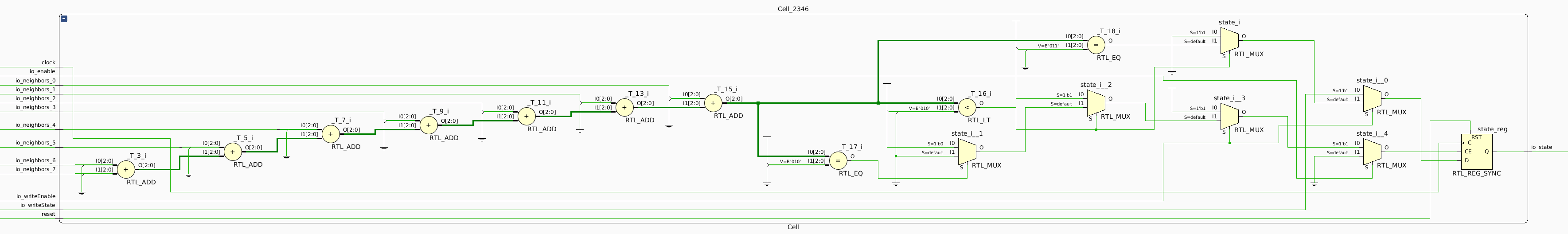
Cell
class Cell extends Module {
  val io = IO(new Bundle {
    val enable = Input(Bool())
    val neighbors = Vec(8, Input(Bool()))
    val state = Output(Bool())
    val writeEnable = Input(Bool())
    val writeState = Input(Bool())
  })
  val state = RegInit(false.B)

  when(io.enable) {
    when(io.writeEnable) {
      state := io.writeState
    }.otherwise {
      val count = io.neighbors.foldRight(0.U(3.W))((x: Bool, y: UInt) => x.asUInt + y)

      when(count < 2.U) {
        state := false.B
      }.elsewhen(count === 2.U) {
        state := state
      }.elsewhen(count === 3.U) {
        state := true.B
      }.otherwise {
        state := false.B
      }
    }
  }

  io.state := state
}
The Cell module inputs are enabled, writeEnabled, writeState, and eight neighbors’ states. When enabled is 1 the cell is either computing its next state at every clock cycle or, when writeEnabled is 1, sets the level of writeState as a new state. When enabled is 0, the cell keeps its state unchanged. The only module output is the current state.
The input/output bundle is followed by the state register with a clock and reset wired implicitly by Chisel. Next is a combinational circuit that computes the GoL rules having neighbors and the own current state bits as input and the new state as an output.
The most interesting line is one that generates a series of adders to compute neighbors’ count. Scala’s foldRight allows expressing this series very succinctly, which shows a glimpse of Chisel’s power. Here is the resulting schematic elaborated by Xilinx Vivado (it is clickable).
Grid
class Grid(val rows: Int, val cols: Int) extends Module {
  val io = IO(new Bundle {
    val readState = Output(Bool())
    val readRow = Input(UInt(log2Ceil(cols).W))
    val readCol = Input(UInt(log2Ceil(rows).W))
    val writeEnable = Input(Bool())
    val writeState = Input(Bool())
    val writeRow = Input(UInt(log2Ceil(cols).W))
    val writeCol = Input(UInt(log2Ceil(rows).W))
  })

  private val cells = Array.fill(rows, cols)(Module(new Cell))
  private var readStates = Seq[(Bool, Bool)]()

  for {
    row <- 0 until rows
    col <- 0 until cols
  } {

    readStates = readStates :+
      (io.readRow === row.U && io.readCol === col.U, cells(row)(col).io.state)

    when (io.writeEnable) {
      val enable = io.writeRow === row.U && io.writeCol === col.U
      cells(row)(col).io.enable := enable
      cells(row)(col).io.writeEnable := enable
      cells(row)(col).io.writeState := io.writeState
    }.otherwise {
      cells(row)(col).io.enable := true.B
      cells(row)(col).io.writeEnable := false.B
      cells(row)(col).io.writeState := false.B
    }
  }

  io.readState := Mux1H(readStates)

  def getNeighbor(row: Int, rowOffset: Int, col: Int, colOffset: Int): (Int, Int) = {
    def wrap(pos: Int, offset: Int, max: Int): Int = {
      if(pos == 0 && offset == -1) {
        max - 1
      } else if (pos == max - 1 && offset == 1) {
        0
      } else {
        pos + offset
      }
    }

    (wrap(row, rowOffset, rows), wrap(col, colOffset, cols))
  }

  for {
    row <- 0 until rows
    col <- 0 until cols
  } {

    val cell = cells(row)(col)
    var i = 0

    for {
      rowOffset <- -1 to 1
      colOffset <- -1 to 1
    } {

      if (rowOffset != 0 || colOffset != 0) {
        val (neighborRow, neighborCol) = getNeighbor(row, rowOffset, col, colOffset)
        cell.io.neighbors(i) := cells(neighborRow)(neighborCol).io.state
        i = i + 1
      }
    }
  }
}
The Grid module integrates cells in a two-dimensional array. The number of rows and columns are the parameters of the grid. The input/output bundle allows for reading and writing cell states addressable by their row and column.
The for loops at the end are particularly notable. They wire up cells’ neighbor states while also wrapping the GoL universe at the edges to form a torus. This code is another excellent example of Chisel’s expressiveness.
GridInit
class GridInit(val rows: Int, val cols: Int, fileName: String) extends Module {
  val io = IO(new Bundle {
    val readState = Output(Bool())
    val readRow = Input(UInt(log2Ceil(cols).W))
    val readCol = Input(UInt(log2Ceil(rows).W))
  })

  def loadPattern(fileName: String): Seq[(Int, Int)] = {
    var pattern = List[(Int, Int)]()
    var row = 0;
    var pattern_cols = 0;

    for (line <- Source.fromFile(fileName).getLines)
      if (!line.startsWith("!")) {
        var col = 0;
        for (c <- line) {
          if (c == 'O')
            pattern = pattern :+ (row, col)

          col = col + 1

          if (pattern_cols < col)
            pattern_cols = col
        }

        row = row + 1
      }

    val pattern_rows = row

    if (pattern_cols + 2 < cols && pattern_rows + 2 < rows) {
      val adjust_cols = (cols - pattern_cols) / 2
      val adjust_rows = (rows - pattern_rows) / 2

      pattern = pattern.map {
        case (row, col) => (row + adjust_rows, col + adjust_cols)
      }
    }

    pattern
  }

  val grid = Module(new Grid(rows, cols))
  val counter = RegInit(0.U(8.W))
  val pattern = loadPattern(fileName)

  when (counter < pattern.length.U) {
    grid.io.writeEnable := true.B
    grid.io.writeState := true.B
    grid.io.writeRow := Mux1H(pattern.zipWithIndex.map {
      case ((row, _), index) => (counter === index.U, row.U)
    })
    grid.io.writeCol := Mux1H(pattern.zipWithIndex.map {
      case ((_, col), index) => (counter === index.U, col.U)
    })

    counter := counter + 1.U
  }.otherwise {
    grid.io.writeEnable := false.B
    grid.io.writeState := false.B
    grid.io.writeRow := 0.U
    grid.io.writeCol := 0.U
  }

  grid.io.readRow := io.readRow
  grid.io.readCol := io.readCol
  io.readState := grid.io.readState
}
The GridInit module initializes the grid with the desired GoL pattern by write-enabling the grid and setting row-column addresses. After the last cell is written, it starts running GoL.
The general-purpose language comes handy to read the file and parse the standard .cells format into a row-column address list.
Elaboration
object Life extends App {
  chisel3.Driver.execute(args, () => new GridInit(48, 64, "p60glidershuttle.cells"))
}
When Scala executes our program, we instruct the Chisel elaboration engine to produce an internal RTL representation called FIRRTL and then transform it into the Verilog source file. Given 64 by 48 grid, Chisel produces stunning 144K lines of Verilog!
VGA
module vga_life(
    input wire sysclk,
    output reg hs, vs,
    output reg [3:0] r, g, b
    );

    parameter FRAME_WIDTH = 1024;
    parameter FRAME_HEIGHT = 768;

    parameter H_FP = 24; // front porch width (pixels)
    parameter H_PW = 136; // sync pulse width (pixels)
    parameter H_MAX = 1344; // total period (pixels)

    parameter V_FP = 3; // front porch width (lines)
    parameter V_PW = 6; // sync pulse width (lines)
    parameter V_MAX = 806; // total period (lines)

    parameter H_POL = 0;
    parameter V_POL = 0;

    wire clk, clk_feedback, pixel;
    reg [11:0] hc, vc;

    PLLE2_BASE #(
        .CLKFBOUT_MULT(7.8),
        .CLKIN1_PERIOD(10.0),
        .CLKOUT0_DIVIDE(12),
        .CLKOUT0_PHASE(0.0)
    ) genclock(
        .CLKOUT0(clk),
        .CLKFBOUT(clk_feedback),
        .CLKIN1(sysclk),
        .PWRDWN(1'b0),
        .RST(1'b0),
        .CLKFBIN(clk_feedback)
    );

    GridInit grid(
        .clock(vs),
        .reset(0),
        .io_readState(pixel),
        .io_readRow(vc[9:4]),
        .io_readCol(hc[9:4])
    );

    initial begin
        hc = 0;
        vc = 0;
    end;

    always @(posedge clk)
        if (hc == (H_MAX - 1))
            hc <= 0;
        else
            hc <= hc + 1;

    always @(posedge clk)
        if ((hc == (H_MAX - 1)) && (vc == (V_MAX - 1)))
            vc <= 0;
        else if (hc == (H_MAX - 1))
            vc <= vc + 1;


    always @(posedge clk)
        if ((hc < FRAME_WIDTH) && (vc < FRAME_HEIGHT)) begin
            r <= {4{pixel}};
            g <= {4{pixel}};
            b <= {4{pixel}};
        end else begin
            r <= 0;
            g <= 0;
            b <= 0;
        end

    always @(posedge clk)
        if (
            (hc >= (H_FP + FRAME_WIDTH - 1)) &&
            (hc < (H_FP + FRAME_WIDTH + H_PW - 1)))
            hs <= H_POL;
        else
            hs <= !H_POL;

    always @(posedge clk)
        if (
            (vc >= (V_FP + FRAME_HEIGHT - 1)) &&
            (vc < (V_FP + FRAME_HEIGHT + V_PW - 1)))
            vs <= V_POL;
        else
            vs <= !V_POL;
endmodule
This simple top-level module written in Verilog ties it all together. It instantiates GridInit and the PLL to generate the clock required for 1024x768 @ 60Hz mode. Each cell takes up a square of 16 by 16 pixels. The grid is clocked with the VGA vertical sync pulse to ensure we apply GoL rules once per screen refresh or at 60 frames per second. The VGA signal forming registers are clocked at much faster 65MHz to produce individual pixels.
FPGA implementation
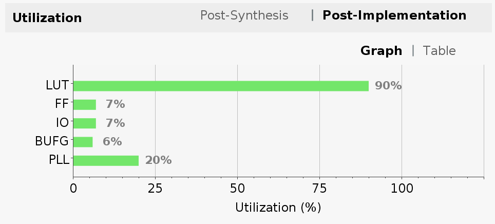
I used Vivado to synthesize and place GoL design on Xilinx Artix-7 XC7A35T-1CSG324 part. Vivado reports 20,800 LUTs available for implementation, and as you can see, 64 by 48 GoL grid takes 90% of all available LUTs.
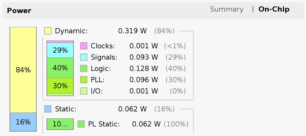
Vivado also estimates the power consumption of our design for a total of 0.381 Watts.
You may have noticed that VGA colors are encoded with 4 bits, also known as RBG444 encoding. I used Digilent’s VGA Pmod to turn it into analog levels required by the VGA.
Seeing is believing
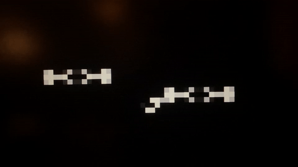
I captured a slow-motion video to be able to see individual GoL generations. At 60 frames per second, it is dizzyingly fast. But more importantly, remember we set the grid’s clock based on how quickly we can render the screen. The propagation delay in the circuit that computes GoL rules determines the true speed limit. This bottleneck poses a more complex problem for placing the cells in the FPGA topology since the length of wires that connect the cell to its neighbors accounts for a meaningful fraction of this delay.
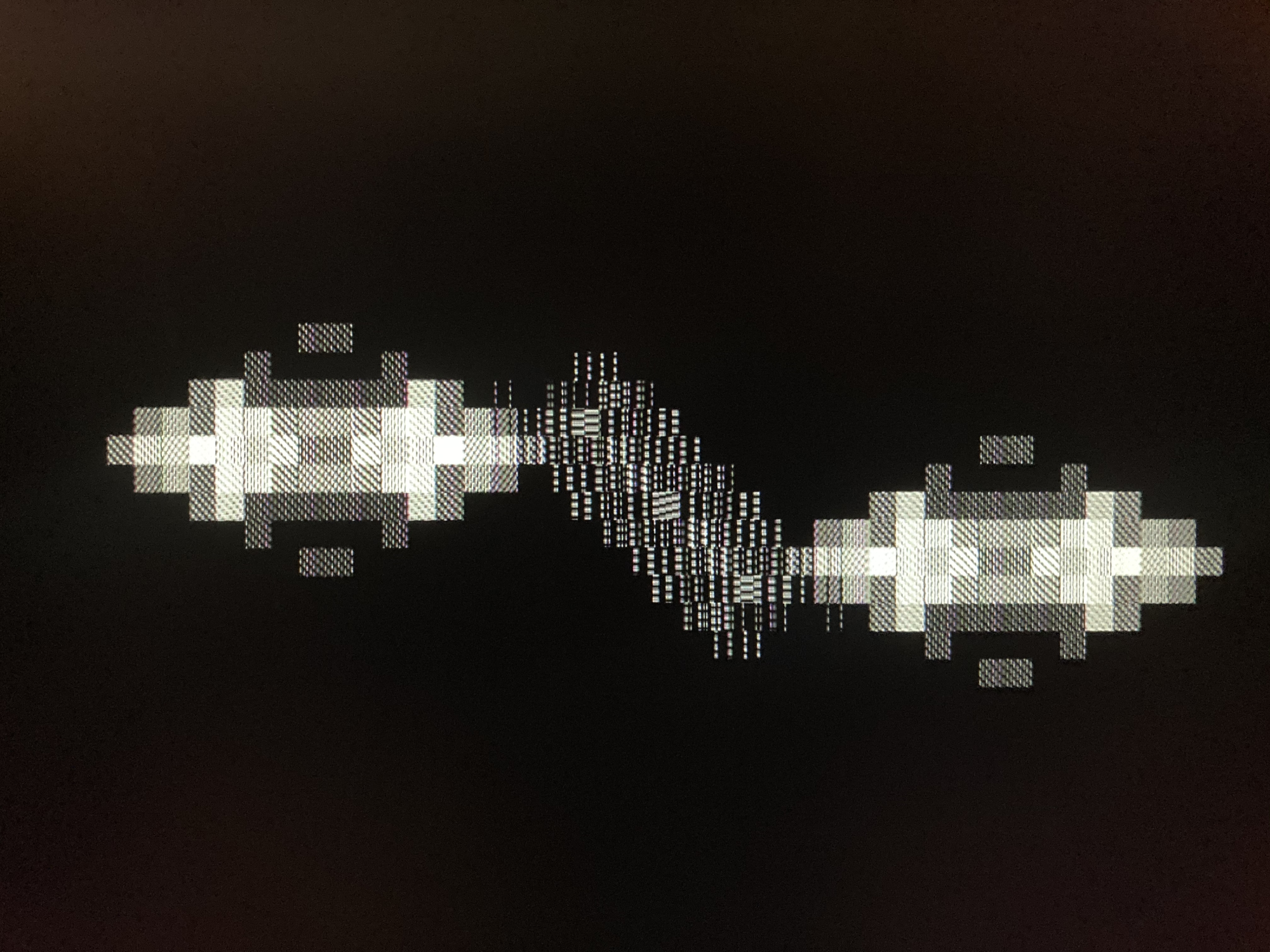
As an experiment, I set the grid’s clock to the board’s external oscillator that runs at 100MHz. When the grid runs at 100 million generations per second, the VGA obviously cannot keep up. Every frame includes pixels from over a million generations creating this beautiful pattern on the screen.
Speed and energy
In conclusion, I wanted to quantify two trivial implementations of GoL. One is running as a software program on modern desktop CPU, and another as implemented in hardware on inexpensive FPGA. First, I will compare the raw speed as latency to compute a new state for a single cell, and second, the estimated energy required for this. Both calculations are “back of the napkin” and only intended to get the feeling for an order of magnitude.
My desktop computer has a six-core processor capable of bursting to 4GHz. This processor has an L1 cache with a 4-cycle latency. We will assume that the GoL universe is small enough to fit entirely in the L1 cache. Thus, the next state’s computation will likely be dominated by L1 accesses to read the eight neighbors’ states and read/write the state itself.
tCPU cell = (4 * 10) * 250ps = 10ns
The FPGA is capable of computing the entire grid containing 3072 cells at 100MHz.
tFPGA cell = 10ns / 3072 = 3.3ps
When it comes to energy, my desktop processor has a thermal design power of 65 Watts. This means it dissipates 65 Joules of energy every second. Let’s assume we utilize all six cores to compute GoL.
ECPU cell = (65J / 6) * 10ns = 108nJ
When I changed the design to use a 100MHz clock for the FPGA grid, Vivado reported a modest power increase to 0.444 Watts.
EFPGA cell = 0.444J * 3.3ps = 1.5pJ